Lab 7: The Advanced Encryption Standard
Introduction & Learning Objectives
In Lab 7, I constructed a hardware accelerator to perform 128-bit AES encryption, taking in a plaintext message and key from the MCU via SPI, and generating and sending the cyphertext from the FPGA. This lab had the following learning objectives:
- Learned to read and implement a complex specification
- Built a nontrivial system on an FPGA that requires thoughtful architecture to fit on the chip
- Designed and implemented an interface to communicate between the FPGA and microprocessor on your MCU
- Learned how to use a logic analyzer to analyze and debug your system
- Gained experience with hardware accelerators
The AES algorithm specifications can be found here and a helpful visualization of the AES algorithm can be found here.
The source code for the project can be found in the associated Github repository.
Design
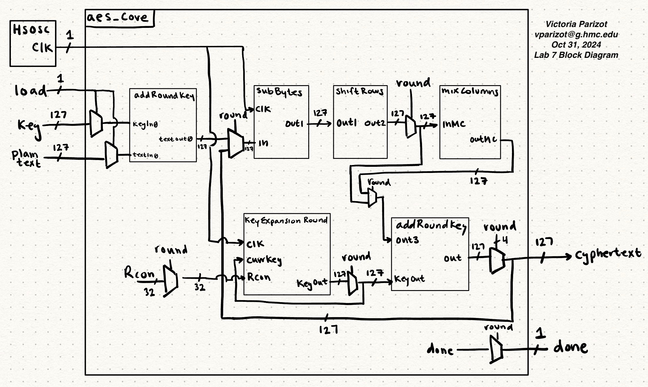
The size limitations on the FPGA makes it so that we are unable to implement AES as a series of combinational logic. As a result, my design reuses modules setting the outputs of a round to be the inputs of the next round.
My design goes through ten rounds, where the round being implemented influences the flow of the signals through the modules. For example, the output for rounds 1-9 passes through the mixColumns module, while for round 10 it does not.
This method allows me to use only one instance of subBytes, shiftRows, mixcolumns, and keyExpansionRound. Important variables are updated and kept in global variables.
I originally opted for not using a FSM for ‘simplicity’, but boy was I wrong. As a result, my design implied many muxes and presented my hardware in an extremely convoluted way, as reflected in the complex block diagram. An FSM would have been a way more organized way to handle the hardware design and varying cases.
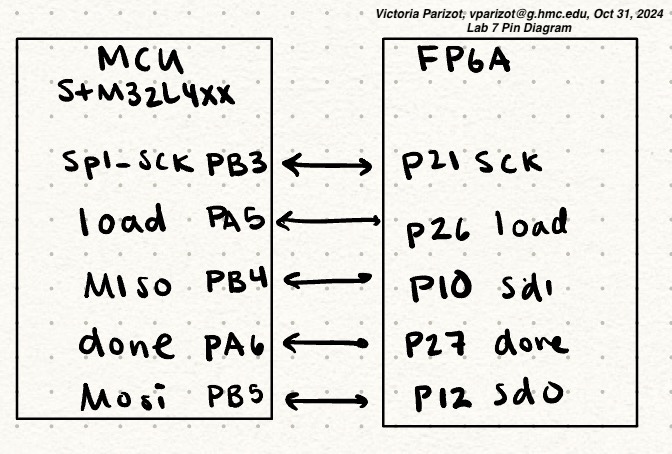
My design is summarized in my Block and Pin diagram below.


Testing & Debugging
Due to the intense recursive nature of this algorithm, once a signal is incorrect, all subsequent signals are incorrect. As a result, it was beneficial to me to text each module and functionality separately, before testing the entire AES through the included AES_Core testbench. I used ModelSim’s wave window to understand the timing of my system, and to isolate my bugs.
My design passes both the AES core and AES SPI simulation testbenches.
After confirming my code works as expected in simulation, is was time to upload my code using Segger and Radiant.
During my hardware integration I ran into a problem of not having enough RAM to map my design onto my FPGA. This was because I had originally made a new module for each round. To solve this issue, I implemented a recurssive design that minimized the number of modules required to go through the 10 rounds.
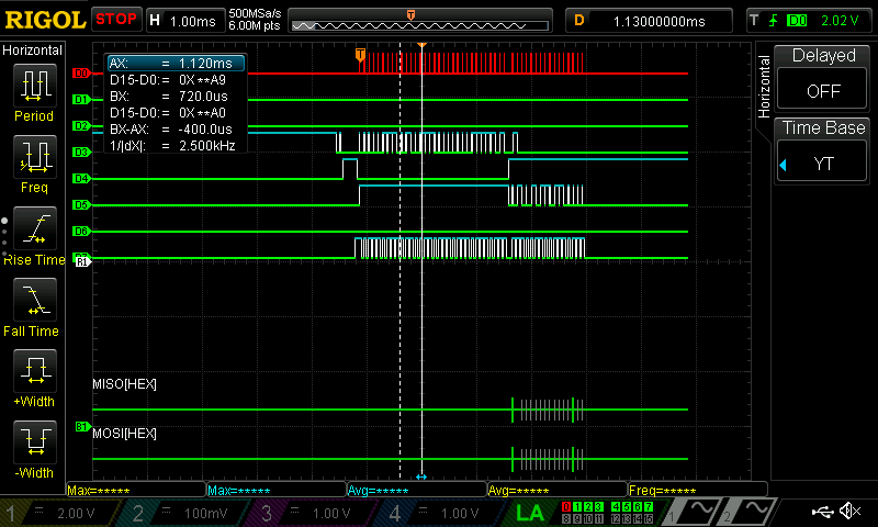
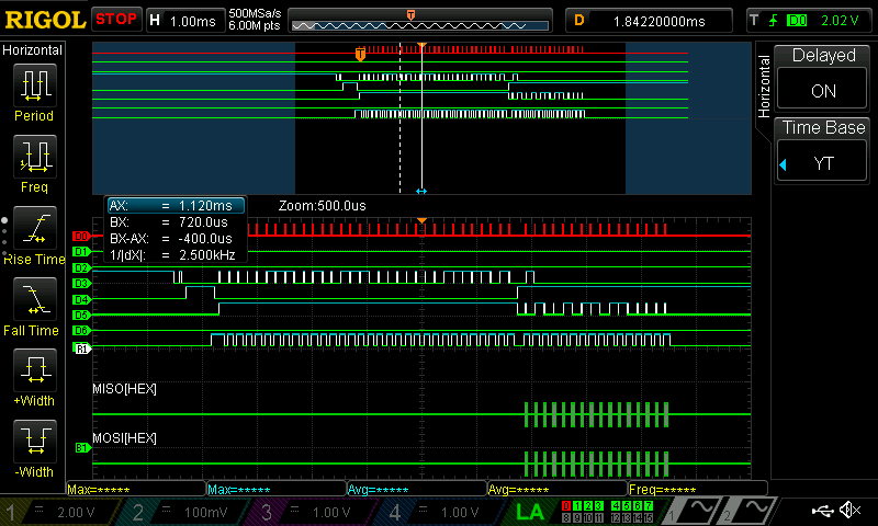
I also hooked up my SPI communication to the logic analyzer, where I set D0 as SCK, D2 as MOSI, D4 as Done, D5 as MISO, and D7 as the chip select. The SPI communication is displayed below:


Conclusion
In lab7.c under the checkAnswer function, we observe that the LEDs on the board reflect the status of AES Encryption and SPI communication. If Lab 7 works as expected, PA9 is driven high.
When running my design, I find that PA9 is driven high. Therefore, Lab 7 meets all the requirements, and took me approximately 30 hours to complete.