Lab 2: Multiplexed 7-Segment Display
Introduction & Learning Objectives
In Lab 2, I implemented a time-multiplexing scheme to drive two seven-segment displays with a single set of FPGA I/O pins. These displayed two independent hexadecimal numbers read from seperate DIP switches and was driven by a single seven-segment decoder HDL module. I also displayed the sum of the numbers on five LEDs. In doing so, I practiced application of transistors and modular verilog.
More information on the lab requirements can be found on the E155 Lab 2 Course Page.
Design
To implement this lab, I had to consider: How should I organize this module in Verilog? How fast should I switch between displays? What transistor type should I use? How do I trigger the transistor? Should I use an anode or cathode display? What resisitor values should I use to protect the FPGA? And so on.
To work my way through these questions, I drew a block diagram. Essentially I pass through two 4 bit signals from the two DIP switches. I then use the on-board high-speed oscillator to act as an selector signal into a 2-to-1 mux that will select a input signal to pass through the single seven-segment decoder HDL module. I then send the decoded signal to both seven-segment cathod displays. I then utilized the selector signal to drive transistors to trigger each display when needed. By using an NPN transistor, I was able to ensure that the current draw/sink on all FPGA pins are below the currents specified in the recommended operating conditions.
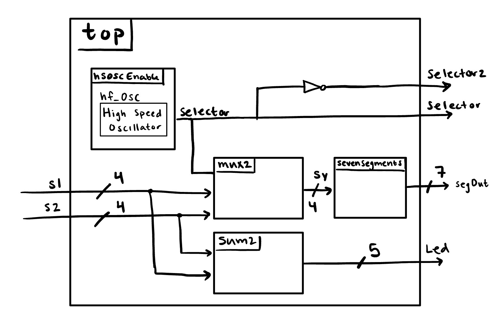
The source code for the project can be found in the associated Github repository.
Testing
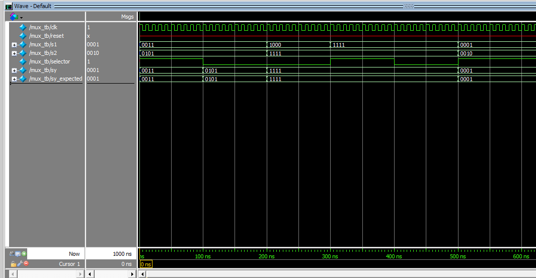
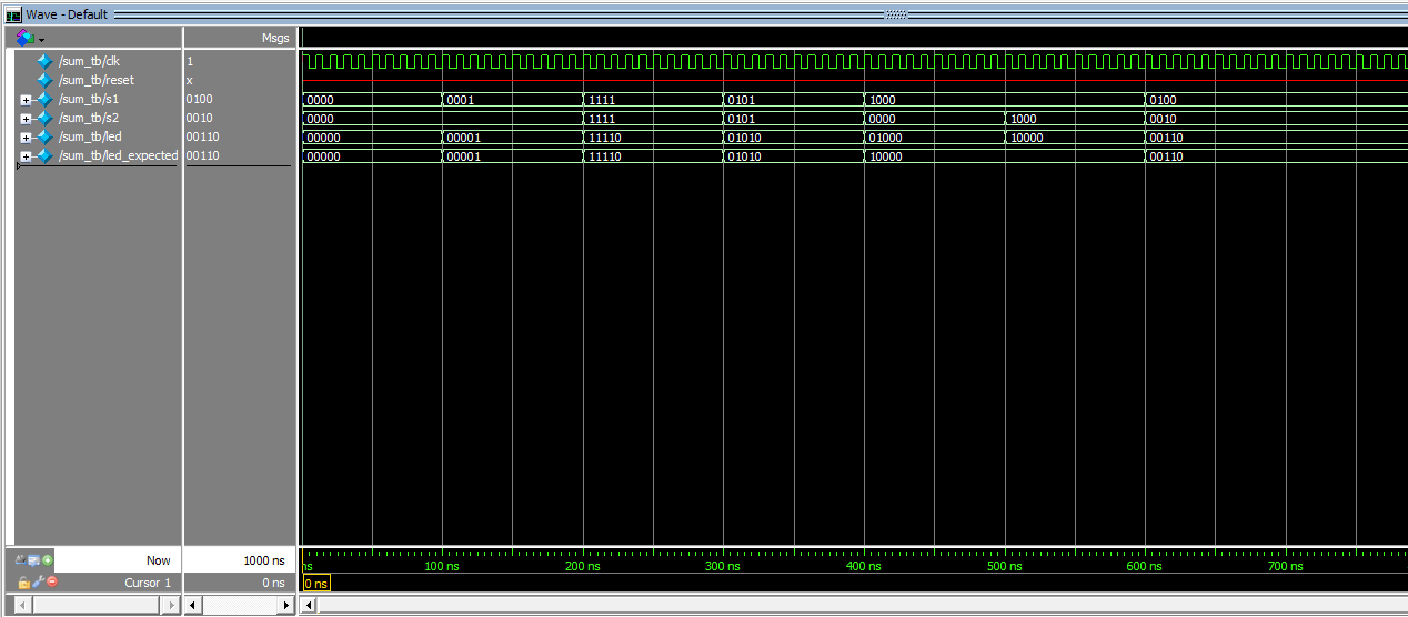
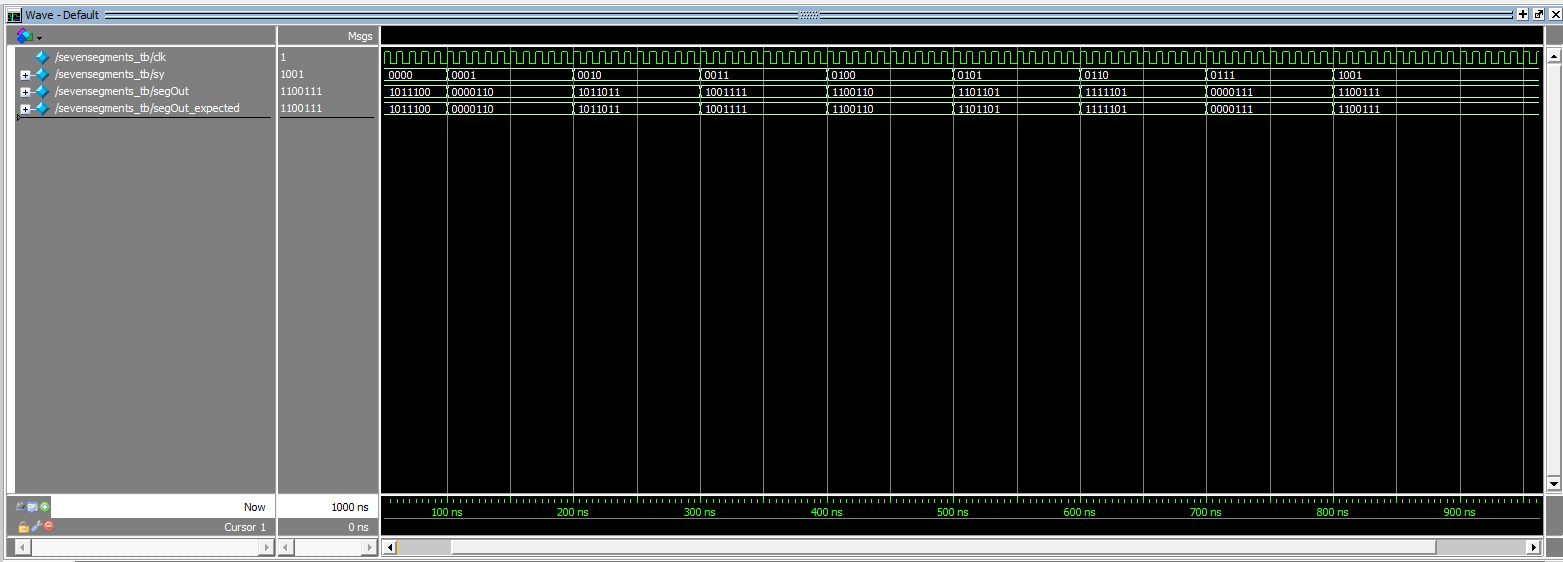
To verify that the design would work as expected, I ran simulations on ModelSim. To do, I instantiated testbenches to test each module. In my testing, I considered edge cases and general cases to examine the behavior of each module. For example, I tested the summing LEDs to ensure that they correctly summed the values of the two DIP switches in binary when they would cause overflow.
The wave forms are below, and the behavior is as expected.
Implementation
After confirming that my design would work in simulation, it was time to wire everything up based on the following circuit schematic. In my design, I used a cathode seven segment display along with NPN transistors for each digit.
Since the display requires substantial current, more than an FPGA output pin can drive, I used an NPN transistor to drive the large current. To calculate the resistor values, I went to the data sheet and found that FPGA pins drive at 3.3 V and 8 mA.
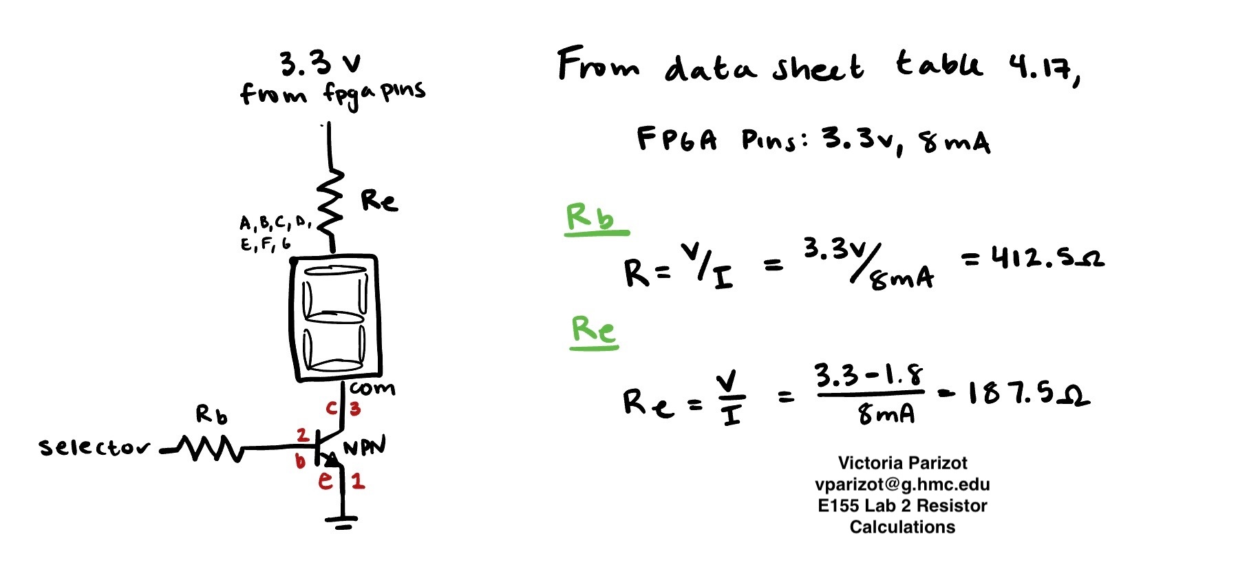
I also implemented the necessary resistors for all led display, based on lab 1 calculations.
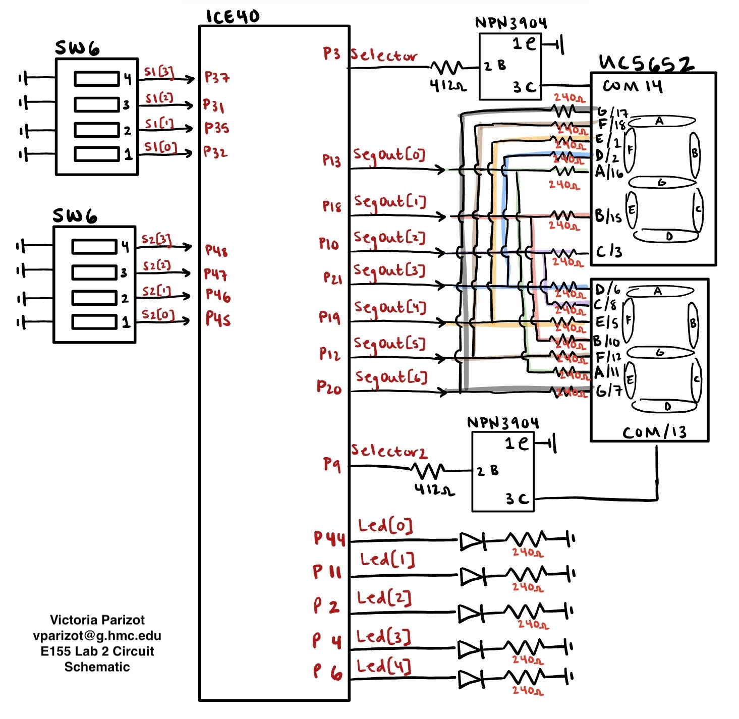
Here is a video of the completed design!
Through trial and error, a suitable switching speed was found so that both sides of the display look like they are on!
Conclusion
Lab 2 provided an introduction to implementing multiplexing in a visual manner. As a result, I grew more familiar with the different type of transistors and calculations for current draw.
Lab 2 meets all the requirements, and took me approximately 13 hours.