
FPGA and MCU Setup and Testing
An exploration and set up of the MCU and FPGA development boards through assembly, programming, simulation, debugging, and hardware implementation.
Introduction & Learning Objectives
In this project, I familiarized myself with the STM32L432KC microcontroller unit (MCU) and UPduino v3.1 field-programmable gate array (FPGA) development boards. This involved assembling the MicroPs protoboard, initial testing, and implementing Verilog to control LEDs and a 7-segment display using Radiant, Segger Embedded Studio, and ModelSim.
More information on the lab requirements can be found on the E155 Lab 1 Course Page.
Development Board: Soldering and Set up
The first step was to assemble the custom printed circuit board which hosts the MCU and FPGA boards. This involved sodering both surface mount technology (SMT) and through hole technology (THT) components, based on the provided BOM.
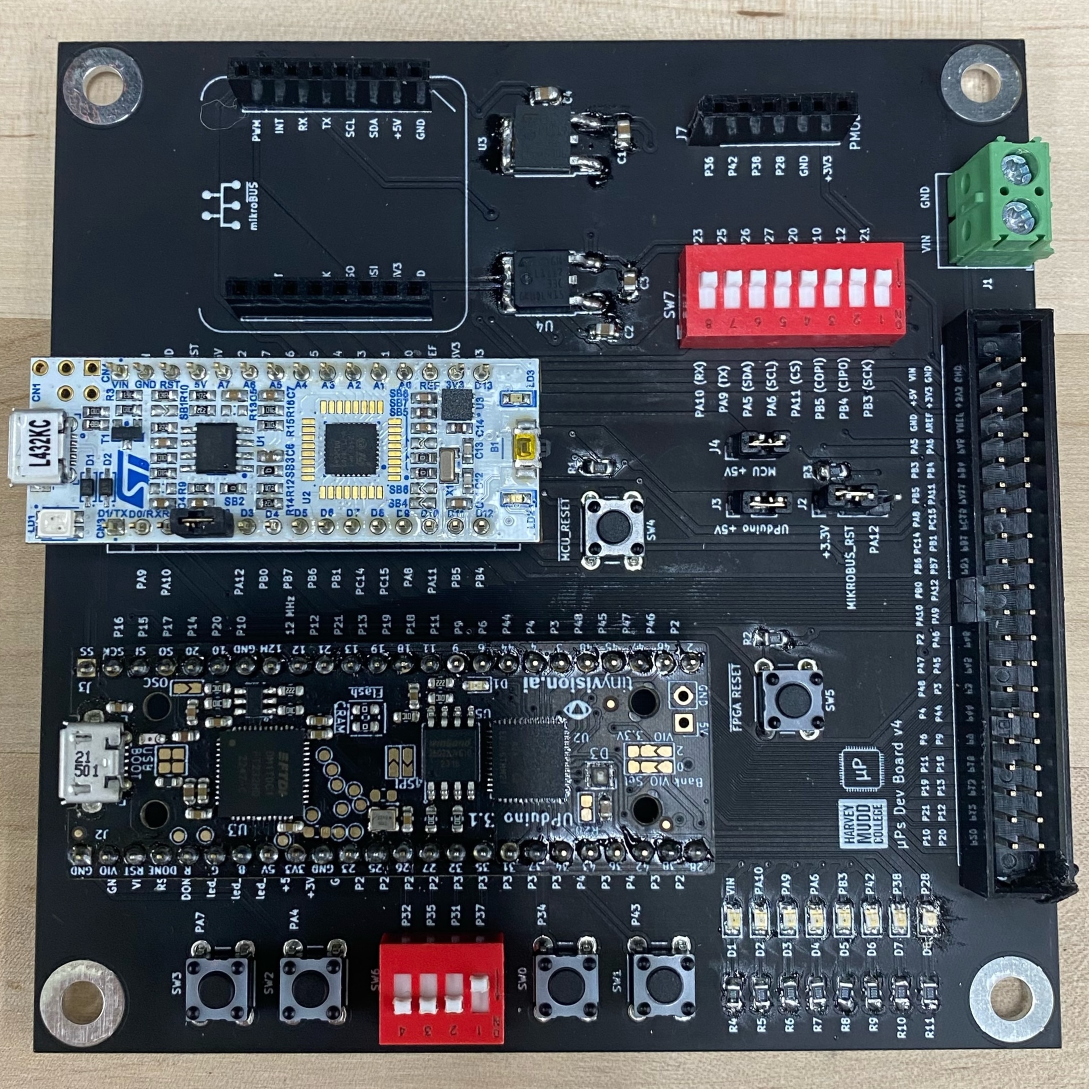
After soldering, it was time to power up and test the board. To do so, I programmed the FPGA using Lattice Radiant and Segger Embedded Studio to toggle LED pins at predetermined frequencies. After confirming my board worked as expected, it was time to implement LEDs and the 7 segment display.
Design & Implementation
Lab Requirements
The next step was to program three LEDs and a seven segment display. The seven segment display is to read four DIP switch signals, s, as a 4-bit binary value and display that value in hexidecimal. The behavior of the LEDs are described by the following tables.
| Signal Name | Signal Type | Description |
|---|---|---|
clk |
input | 48 MHz clock on FPGA |
s[3:0] |
input | the four DIP switches (on the board, SW6) |
led[2:0] |
output | 3 LEDs (you may use the on-board LEDs) |
seg[6:0] |
output | the segments of a common-anode 7-segment display |
The following tables define the relationship of the LEDs to the switches and clock.
S1 |
S0 |
led[0] |
|---|---|---|
| 0 | 0 | OFF |
| 0 | 1 | ON |
| 1 | 0 | ON |
| 1 | 1 | OFF |
S3 |
S2 |
led[1] |
|---|---|---|
| 0 | 0 | OFF |
| 0 | 1 | OFF |
| 1 | 0 | OFF |
| 1 | 1 | ON |
led[2] |
|---|
| Blink at 2.4 Hz |
Design
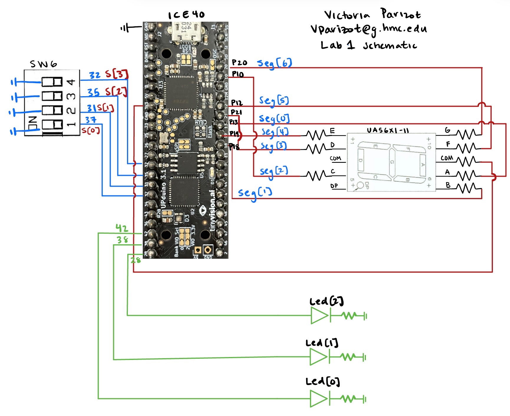
To organize my thoughts I used a simple block diagram to map the logic.

Led Logic Design
The truth tables revealed that led[0] behaves as an XOR gate with inputs S1 and S0 and that led[1] behaves as an AND gate with inputs S3 and S2.
To have led[2] to blink at 2.4 Hz, I utilized the internal 48 GHz high speed oscillator from the HSOSC Library. A frequency of 2.4 Hz would have a full cycle of 0.4167 second. Dividing this by the frequency of the internal oscillator, I got that a full cycle would require $2*10^7$ ticks. To achieve a duty cycle of 50%, I implemented a flip flop that switched led[2] every $10^7$ clicks.
Seven Segment Logic Design
To interface the seven segment display with the board, I conferred with the datasheet to determine resistor values.
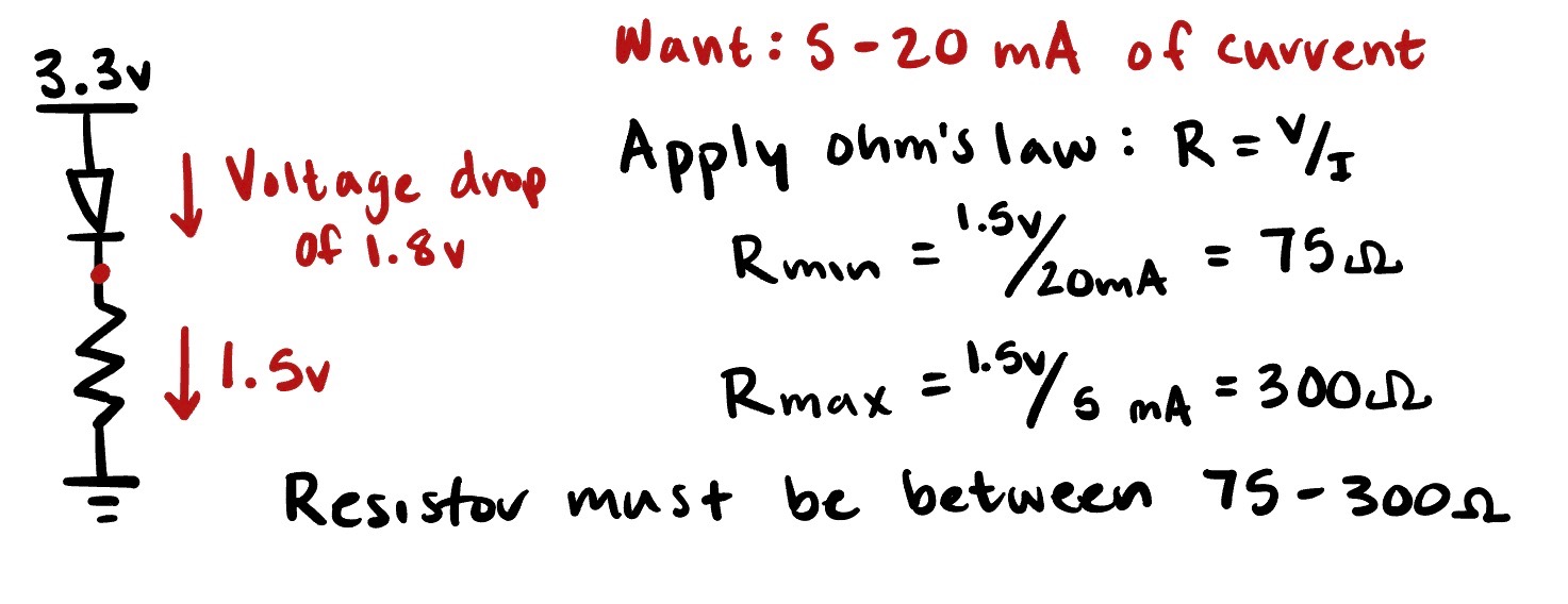
I opted to use resistor values of 240 ohms, producing 6.25 mA of current.
A wiring schematic is shown below.
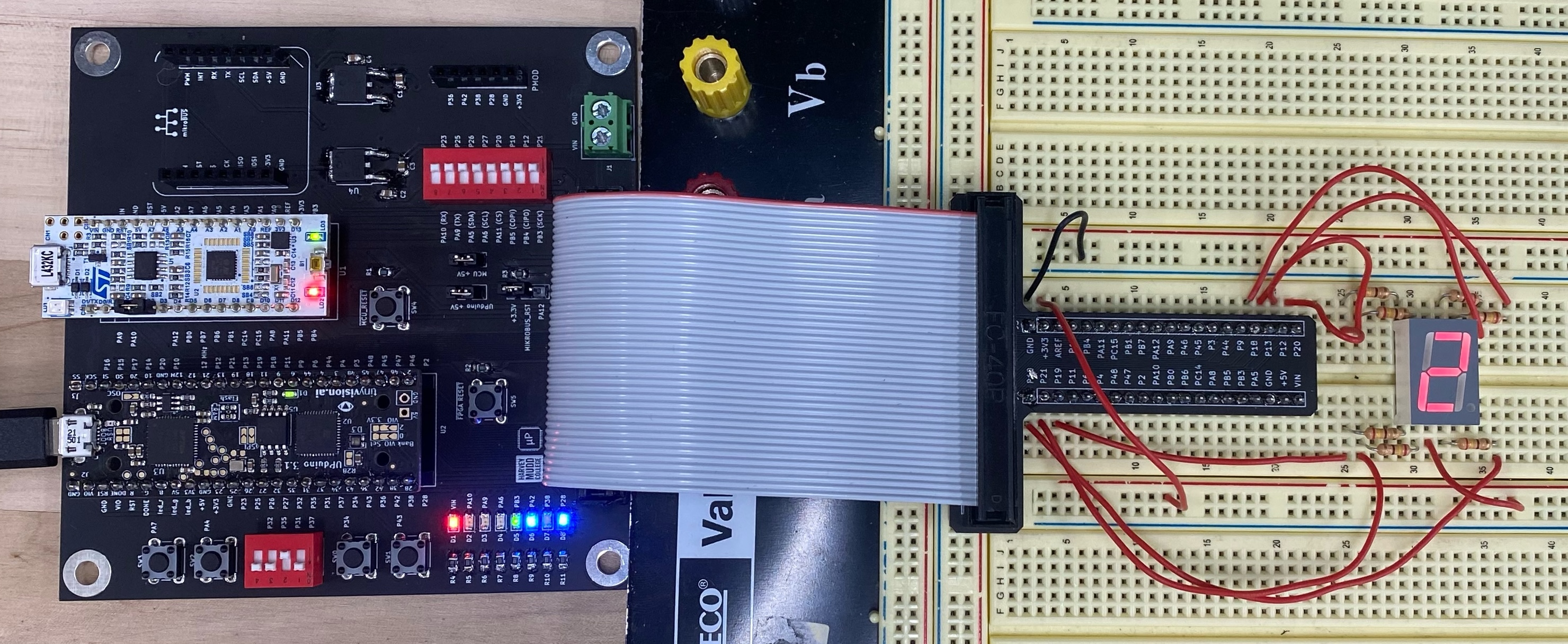
Here is a photo of the implemented design!
Testing
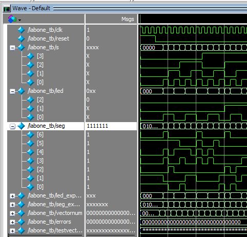
To verify that the design would work as expected, I ran simulations on ModelSim. To do, I instantiated a test bench that would test all 16 possible inputs of the dip switch to ensure the LED and seven segment display output as expected.
I tested the blinking led[2] with the oscilliscope to confirm it had a frequency of 2.4 hz.
![Frequency verification of led[2]](/assets/images/lab1/240HzLed%5B2%5D.png)
Conclusion
In all, this project offered a cohesive introduction to the work flow for the coming labs. I was able to practice my sodering technique, interfacing with different software, assigning pins, and testing my design with ModelSim.
The design meets all the requirements.